- 您现在的位置:买卖IC网 > Sheet目录2000 > IDTSSTE32882KA1AKG (IDT, Integrated Device Technology Inc)IC REGISTERING CLK DRIVER 176BGA
1.25V/1.35V/1.5V REGISTERING CLOCK DRIVER WITH PARITY TEST AND QUAD CHIP SELECT
16
SSTE32882KA1
7314/8
THE INFORMATION IN THIS DOCUMENT IS SUBJECT TO CHANGE WITHOUT NOTICE
SSTE32882KA1
1.25V/1.35V/1.5V REGISTERING CLOCK DRIVER WITH PARITY TEST AND QUAD CHIP SELECT
COMMERCIAL TEMPERATURE RANGE
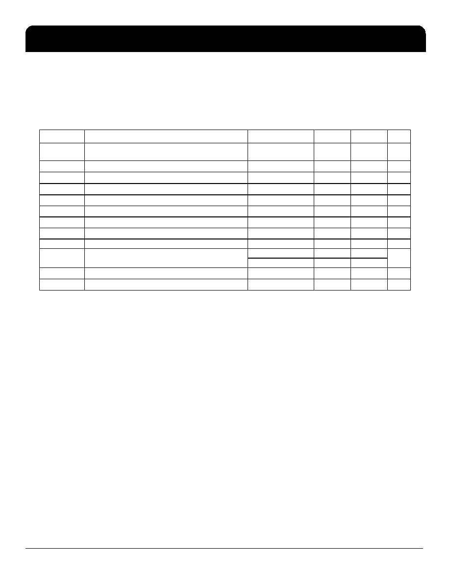
Absolute Maximum Ratings
Stresses greater than those listed under ABSOLUTE MAXIMUM RATINGS may cause permanent damage to the device. This
is a stress rating only and functional operation of the device at these or any other conditions above those indicated in the
operational sections of this specification is not implied. Exposure to absolute maximum rating conditions for extended periods
may affect reliability
DC and AC Specifications
The SSTE32882KA1 parametric values are specified for the device default control word settings, unless otherwise stated. Note that
RC10 setting does not affect any of the paramteric values.
Symbol
Parameter
Conditions
Min
Max
Unit
AVDD, PVDD,
VDD
Supply voltage
–0.4
+1.975
V
VI
Receiver input voltage1
1
The input and output negative-voltage ratings may be exceeded if the input and output clamp-current ratings are
observed. This value is limited to 1.975 V maximum.
–0.4
VDD +0.5
V
VREF
Reference voltage
–0.4
VDD +0.5
V
VO
Driver output voltage1
–0.4
VDD +0.5
V
IIK
Input clamp current
VI < 0 or VI > VDD
-50
mA
IOK
Output clamp current
VO < 0 or VO > VDD
±50
mA
IO
Continuous output current
0 < VO < VDD
±50
mA
ICCC
Continuous current through each VDD or GND pin
±100
mA
TSTG
Storage temperature
–65
+150
°C
R
θJA
Package Thermal Impedance, Junction-to-Ambient2
2
The package thermal impedance is calculated in accordance with JESD51-2.
0m/s Airflow
43.8
°C/W
1m/s Airflow
35.5
R
θJB
Package Thermal Impedance, Junction-to-Board2
22
°C/W
R
θJC
Package Thermal Impedance, Junction-to-Case2
16.2
°C/W
发布紧急采购,3分钟左右您将得到回复。
相关PDF资料
ISD1750SYR
IC VOICE REC/PLAY 50SEC 28-SOIC
ISD5008EYI
IC VOICE REC/PLAY 4-8MIN 28-TSOP
ISL12008IB8Z
IC RTC I2C LO-POWER 8-SOIC
ISL12020MIRZ-T7A
IC RTC/CALENDAR TEMP SNSR 20DFN
ISL12022IBZ-T7A
IC RTC/CALENDAR TEMP SNSR 8SOIC
ISL12022MAIBZ
IC RTC/CALENDAR TEMP SNSR 20SOIC
ISL12022MIBZ-T7A
IC RTC/CALENDAR TEMP SNSR 20SOIC
ISL12022MIBZR5421
IC RTC/CALENDAR TEMP SNSR 20SOIC
相关代理商/技术参数
IDTSSTE32882KA1AKG8
制造商:Integrated Device Technology Inc 功能描述:IC REGISTERING CLK DRIVER 176BGA
IDTSSTUB32866BHLF
功能描述:IC BUFFER 25BIT CONF REG 96LFBGA RoHS:是 类别:集成电路 (IC) >> 接口 - 专用 系列:- 特色产品:NXP - I2C Interface 标准包装:1 系列:- 应用:2 通道 I²C 多路复用器 接口:I²C,SM 总线 电源电压:2.3 V ~ 5.5 V 封装/外壳:16-TSSOP(0.173",4.40mm 宽) 供应商设备封装:16-TSSOP 包装:剪切带 (CT) 安装类型:表面贴装 产品目录页面:825 (CN2011-ZH PDF) 其它名称:568-1854-1
IDTSSTUB32S869AHLF
功能描述:IC REGISTERED BUFFER 150-TFBGA RoHS:是 类别:集成电路 (IC) >> 接口 - 信号缓冲器,中继器,分配器 系列:- 标准包装:160 系列:- 类型:转发器 Tx/Rx类型:以太网 延迟时间:- 电容 - 输入:- 电源电压:2.37 V ~ 2.63 V 电流 - 电源:60mA 安装类型:表面贴装 封装/外壳:64-TQFP 裸露焊盘 供应商设备封装:64-TQFP-EP(10x10) 包装:托盘 其它名称:Q5134101
IDTSSTUB32S869AHLFT
功能描述:IC REGISTERED BUFFER 150-TFBGA RoHS:是 类别:集成电路 (IC) >> 接口 - 信号缓冲器,中继器,分配器 系列:- 标准包装:160 系列:- 类型:转发器 Tx/Rx类型:以太网 延迟时间:- 电容 - 输入:- 电源电压:2.37 V ~ 2.63 V 电流 - 电源:60mA 安装类型:表面贴装 封装/外壳:64-TQFP 裸露焊盘 供应商设备封装:64-TQFP-EP(10x10) 包装:托盘 其它名称:Q5134101
IDTSSTVF16857AGLF
功能描述:IC DDR REGISTER 48-TSSOP RoHS:是 类别:集成电路 (IC) >> 接口 - 专用 系列:- 标准包装:3,000 系列:- 应用:PDA,便携式音频/视频,智能电话 接口:I²C,2 线串口 电源电压:1.65 V ~ 3.6 V 封装/外壳:24-WQFN 裸露焊盘 供应商设备封装:24-QFN 裸露焊盘(4x4) 包装:带卷 (TR) 安装类型:表面贴装 产品目录页面:1015 (CN2011-ZH PDF) 其它名称:296-25223-2
IDTSTAC9200X3NAEB1X
功能描述:IC AUDIO CODEC 2CH HD 32-QFN RoHS:是 类别:集成电路 (IC) >> 接口 - 编解码器 系列:- 标准包装:2,500 系列:- 类型:立体声音频 数据接口:串行 分辨率(位):18 b ADC / DAC 数量:2 / 2 三角积分调变:是 S/N 比,标准 ADC / DAC (db):81.5 / 88 动态范围,标准 ADC / DAC (db):82 / 87.5 电压 - 电源,模拟:2.6 V ~ 3.3 V 电压 - 电源,数字:1.7 V ~ 3.3 V 工作温度:-40°C ~ 85°C 安装类型:表面贴装 封装/外壳:48-WFQFN 裸露焊盘 供应商设备封装:48-TQFN-EP(7x7) 包装:带卷 (TR)
IDTSTAC9200X3NAEB1XR
功能描述:IC AUDIO CODEC 2CH HD 32-QFN RoHS:是 类别:集成电路 (IC) >> 接口 - 编解码器 系列:- 标准包装:2,500 系列:- 类型:立体声音频 数据接口:串行 分辨率(位):18 b ADC / DAC 数量:2 / 2 三角积分调变:是 S/N 比,标准 ADC / DAC (db):81.5 / 88 动态范围,标准 ADC / DAC (db):82 / 87.5 电压 - 电源,模拟:2.6 V ~ 3.3 V 电压 - 电源,数字:1.7 V ~ 3.3 V 工作温度:-40°C ~ 85°C 安装类型:表面贴装 封装/外壳:48-WFQFN 裸露焊盘 供应商设备封装:48-TQFN-EP(7x7) 包装:带卷 (TR)
IDTSTAC9200X3TAEB1X
功能描述:IC AUDIO CODEC 2CH HD 48-LQFP RoHS:是 类别:集成电路 (IC) >> 接口 - 编解码器 系列:- 标准包装:2,500 系列:- 类型:立体声音频 数据接口:串行 分辨率(位):18 b ADC / DAC 数量:2 / 2 三角积分调变:是 S/N 比,标准 ADC / DAC (db):81.5 / 88 动态范围,标准 ADC / DAC (db):82 / 87.5 电压 - 电源,模拟:2.6 V ~ 3.3 V 电压 - 电源,数字:1.7 V ~ 3.3 V 工作温度:-40°C ~ 85°C 安装类型:表面贴装 封装/外壳:48-WFQFN 裸露焊盘 供应商设备封装:48-TQFN-EP(7x7) 包装:带卷 (TR)